1. Material Principles and Architectural Qualities of Alumina Ceramics
1.1 Crystallographic and Compositional Basis of α-Alumina
(Alumina Ceramic Substrates)
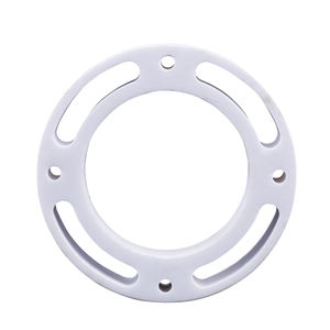
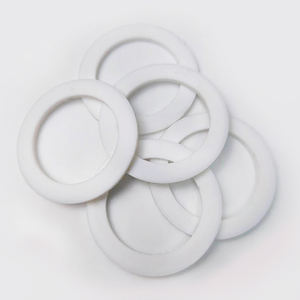
Alumina ceramic substrates, primarily composed of aluminum oxide (Al ₂ O TWO), function as the foundation of modern digital packaging because of their outstanding balance of electric insulation, thermal stability, mechanical toughness, and manufacturability.
One of the most thermodynamically steady stage of alumina at heats is diamond, or α-Al ₂ O ₃, which crystallizes in a hexagonal close-packed oxygen latticework with aluminum ions occupying two-thirds of the octahedral interstitial sites.
This dense atomic setup imparts high firmness (Mohs 9), excellent wear resistance, and strong chemical inertness, making α-alumina ideal for harsh operating settings.
Business substratums commonly contain 90– 99.8% Al Two O FOUR, with minor enhancements of silica (SiO ₂), magnesia (MgO), or unusual planet oxides used as sintering aids to promote densification and control grain growth throughout high-temperature handling.
Greater pureness qualities (e.g., 99.5% and over) display remarkable electrical resistivity and thermal conductivity, while lower pureness variations (90– 96%) provide cost-effective remedies for less requiring applications.
1.2 Microstructure and Flaw Engineering for Electronic Integrity
The efficiency of alumina substratums in electronic systems is critically dependent on microstructural harmony and defect reduction.
A fine, equiaxed grain structure– typically varying from 1 to 10 micrometers– guarantees mechanical integrity and minimizes the chance of crack propagation under thermal or mechanical anxiety.
Porosity, particularly interconnected or surface-connected pores, should be minimized as it degrades both mechanical stamina and dielectric performance.
Advanced handling techniques such as tape casting, isostatic pushing, and regulated sintering in air or regulated atmospheres enable the manufacturing of substratums with near-theoretical density (> 99.5%) and surface roughness listed below 0.5 µm, crucial for thin-film metallization and cord bonding.
Furthermore, pollutant segregation at grain boundaries can bring about leakage currents or electrochemical movement under predisposition, requiring rigorous control over raw material purity and sintering problems to ensure lasting reliability in damp or high-voltage settings.
2. Manufacturing Processes and Substratum Fabrication Technologies
( Alumina Ceramic Substrates)
2.1 Tape Spreading and Environment-friendly Body Handling
The production of alumina ceramic substrates begins with the prep work of a highly distributed slurry consisting of submicron Al two O six powder, natural binders, plasticizers, dispersants, and solvents.
This slurry is refined by means of tape spreading– a continuous method where the suspension is spread over a relocating carrier movie utilizing a precision medical professional blade to accomplish uniform density, typically between 0.1 mm and 1.0 mm.
After solvent dissipation, the resulting “eco-friendly tape” is adaptable and can be punched, pierced, or laser-cut to create via holes for upright affiliations.
Several layers may be laminated flooring to produce multilayer substratums for intricate circuit integration, although most of industrial applications utilize single-layer configurations because of set you back and thermal expansion factors to consider.
The green tapes are after that very carefully debound to remove organic ingredients through regulated thermal disintegration before final sintering.
2.2 Sintering and Metallization for Circuit Assimilation
Sintering is performed in air at temperatures in between 1550 ° C and 1650 ° C, where solid-state diffusion drives pore elimination and grain coarsening to achieve complete densification.
The straight contraction throughout sintering– normally 15– 20%– need to be specifically anticipated and compensated for in the style of eco-friendly tapes to make sure dimensional accuracy of the final substrate.
Following sintering, metallization is put on develop conductive traces, pads, and vias.
2 primary techniques control: thick-film printing and thin-film deposition.
In thick-film innovation, pastes having metal powders (e.g., tungsten, molybdenum, or silver-palladium alloys) are screen-printed onto the substratum and co-fired in a reducing environment to develop durable, high-adhesion conductors.
For high-density or high-frequency applications, thin-film procedures such as sputtering or dissipation are utilized to down payment attachment layers (e.g., titanium or chromium) followed by copper or gold, making it possible for sub-micron patterning using photolithography.
Vias are filled with conductive pastes and fired to develop electrical affiliations in between layers in multilayer layouts.
3. Useful Characteristics and Efficiency Metrics in Electronic Systems
3.1 Thermal and Electrical Habits Under Operational Tension
Alumina substratums are prized for their favorable combination of moderate thermal conductivity (20– 35 W/m · K for 96– 99.8% Al ₂ O ₃), which makes it possible for effective heat dissipation from power tools, and high volume resistivity (> 10 ¹⁴ Ω · cm), guaranteeing very little leakage current.
Their dielectric consistent (εᵣ ≈ 9– 10 at 1 MHz) is steady over a vast temperature level and regularity array, making them ideal for high-frequency circuits as much as several ghzs, although lower-κ materials like aluminum nitride are favored for mm-wave applications.
The coefficient of thermal development (CTE) of alumina (~ 6.8– 7.2 ppm/K) is fairly well-matched to that of silicon (~ 3 ppm/K) and particular packaging alloys, decreasing thermo-mechanical tension during gadget procedure and thermal biking.
Nevertheless, the CTE mismatch with silicon remains a problem in flip-chip and direct die-attach configurations, usually needing certified interposers or underfill materials to alleviate exhaustion failing.
3.2 Mechanical Toughness and Ecological Longevity
Mechanically, alumina substrates display high flexural toughness (300– 400 MPa) and exceptional dimensional stability under load, allowing their use in ruggedized electronic devices for aerospace, automotive, and industrial control systems.
They are resistant to resonance, shock, and creep at elevated temperatures, keeping structural integrity approximately 1500 ° C in inert environments.
In humid atmospheres, high-purity alumina reveals very little dampness absorption and exceptional resistance to ion movement, making sure long-lasting reliability in outside and high-humidity applications.
Surface area firmness also safeguards versus mechanical damages during handling and assembly, although care needs to be taken to stay clear of edge cracking because of intrinsic brittleness.
4. Industrial Applications and Technological Influence Throughout Sectors
4.1 Power Electronic Devices, RF Modules, and Automotive Solutions
Alumina ceramic substrates are ubiquitous in power electronic components, consisting of protected gate bipolar transistors (IGBTs), MOSFETs, and rectifiers, where they give electric isolation while helping with warm transfer to warmth sinks.
In superhigh frequency (RF) and microwave circuits, they function as provider platforms for hybrid integrated circuits (HICs), surface area acoustic wave (SAW) filters, and antenna feed networks as a result of their secure dielectric residential or commercial properties and reduced loss tangent.
In the auto industry, alumina substrates are used in engine control devices (ECUs), sensing unit bundles, and electrical car (EV) power converters, where they endure high temperatures, thermal cycling, and direct exposure to harsh liquids.
Their integrity under harsh conditions makes them vital for safety-critical systems such as anti-lock stopping (ABS) and progressed vehicle driver assistance systems (ADAS).
4.2 Medical Instruments, Aerospace, and Arising Micro-Electro-Mechanical Systems
Beyond customer and industrial electronics, alumina substrates are used in implantable medical devices such as pacemakers and neurostimulators, where hermetic sealing and biocompatibility are extremely important.
In aerospace and defense, they are made use of in avionics, radar systems, and satellite interaction modules due to their radiation resistance and security in vacuum cleaner atmospheres.
Furthermore, alumina is progressively used as a structural and shielding platform in micro-electro-mechanical systems (MEMS), including pressure sensing units, accelerometers, and microfluidic devices, where its chemical inertness and compatibility with thin-film processing are helpful.
As electronic systems remain to demand greater power thickness, miniaturization, and reliability under severe problems, alumina ceramic substrates stay a cornerstone product, linking the void between efficiency, price, and manufacturability in innovative electronic packaging.
5. Vendor
Alumina Technology Co., Ltd focus on the research and development, production and sales of aluminum oxide powder, aluminum oxide products, aluminum oxide crucible, etc., serving the electronics, ceramics, chemical and other industries. Since its establishment in 2005, the company has been committed to providing customers with the best products and services. If you are looking for high quality alumina oxide, please feel free to contact us. (nanotrun@yahoo.com)
Tags: Alumina Ceramic Substrates, Alumina Ceramics, alumina
All articles and pictures are from the Internet. If there are any copyright issues, please contact us in time to delete.
Inquiry us